| SHIFTIN | Example |
SHIFTIN DPin, CPin, ShiftMode, ByteVar {\Count} {, SpeedMult}
Function
Shift data out to a synchronous serial device.
Explanation
SHIFTIN and SHIFTOUT provide an easy method of connecting to
synchronous serial devices. Synchronous serial differs from asynchronous serial
(like SERIN and SEROUT) in that the timing of data bits (on a data
line) is specified in relationship to clock pulses (on a clock line). Data bits
may be valid after the rising or falling edge of the clock line. This kind of
serial protocol is commonly used by controller peripherals like ADCs, DACs, clocks,
memory devices, etc.
At their heart, synchronous-serial devices are essentially shift-registers; trains of flip-flops that pass data bits along in a bucket brigade fashion to a single data output pin. Another bit is output each time the appropriate edge (rising or falling, depending on the device) appears on the clock line.
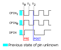
The SHIFTIN instruction first forces the clock pin (CPin) to output mode and the data pin (DPin) to input mode. Then, SHIFTIN either reads the data pin and generates a clock pulse (PRE mode) or generates a clock pulse then reads the data pin (POST mode). Clock pulses are generated by inverting the state of CPin, allowing the programmer to determine CPin behavior by presetting the pin to the opposite state prior to the call. SHIFTIN continues to generate clock pulses and read the data pin for as many data bits as are required.
Making SHIFTIN work with a particular device is a matter of matching the mode and number of bits to that device's protocol. Most manufacturers use a timing diagram to illustrate the relationship of clock and data. Items to look for include: 1) which bit of the data arrives first; most significant bit (MSB) or least significant bit (LSB) and 2) is the first data bit ready before the first clock pulse (PRE) or before the second clock pulse (POST). The table below shows the values and symbols available for the ShiftMode parameter.
| Symbol | Value | Meaning |
| MSBPRE | 0 | Data is MSB-first; sample bits before clock pulse |
| LSBPRE | 1 | Data is lsb-first; sample bits before clock pulse |
| MSBPOST | 2 | Data is MSB-first; sample bits after clock pulse |
| LSBPOST | 3 | Data is LSB-first; sample bits after clock pulse |
SHIFTIN Timing
| T0 - T1, T1 - T2, ... | ~ 6 µs |
| Transmission Rate | ~ 83 kBits/Sec |
Here is a simple example:
SHIFTIN RC.0, RC.1, MSBPRE, result
Here, the SHIFTIN instruction will read pin RC.0 (Dpin) and will generate a clock signal on RA.1 (Cpin). The data that arrives on the Dpin depends on the device connected to it. Let's say, for example, that a shift register is connected and has a value of $AF (%10101111) waiting to be sent. Additionally, let's assume that the shift register sends out the most significant bit first, and the first bit is on the Dpin before the first clock pulse (MSBPRE). The SHIFTIN instruction above will generate eight clock pulses and sample the Dpin eight times. Afterward, the result variable will contain the value $AF.
Some devices return more than eight bits. For example, the LTC1298 is a 12-bit ADC. To retrieve data from the LTC1298 would require two SHIFTIN calls to retrieve the 12-bit result.
  LOW CS
  SHIFTOUT Dio, Clk, LSBFIRST, config\4         ' send config bits
  SHIFTIN  Dio, Clk, MSBPOST, resultHi\4        ' get data (upper nibble)
  SHIFTIN  Dio, Clk, MSBPOST, resultLo\8        ' get data (lower byte)
  HIGH CS
Related instructions: SHIFTOUT
Related project: Thermometer